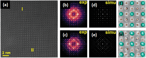

 Atomic‐resolution imaging of halide perovskites (HPs) using transmission electron microscopy (TEM) is challenging because of the sensitivity of their structures to the electron beam. In this article, recent achievements in this area are reviewed, covering both all‐inorganic and organic–inorganic hybrid HPs, with an emphasis on the specific imaging conditions that have proven to be effective in avoiding electron beam‐induced structural damage. The discussion focusses on the total electron dose that HPs can bear before being damaged and the effects of different imaging modes, accelerating voltages, and temperatures. The crucial role of a direct‐detection electron‐counting camera in reducing the required electron dose is outlined, which is indispensable for imaging extremely sensitive organic–inorganic hybrid perovskites. In addition to reviewing published works, the results of initial attempts to perform atomic‐resolution elemental mapping for an all‐inorganic HP and image a hybrid HP using scanning TEM are introduced. The preparation of a TEM specimen from macroscopic crystals or devices of HPs, which is very important for practical applications but has not yet received attention, is also discussed. This article aims to provide guidance on the acquisition of atomic‐resolution TEM images of HPs and inspire the development of more imaging technologies for sensitive materials.